Quick Link
- Dept. of El./Eng., Kyoto Univ.
- Grant-in-Aid forScientific Research from the Ministry of Education, Culture,Sports, Science and Technology (MEXT) of Japan, Innovative Area “Nano Spin Conversion Science”
- Grant-in-Aid for Scientific Research (S) “Semiconductor Spincurrentronics”
- Evaluation and Verification Results
- Reserch Abstract
-
CONTACT
- Post Code: 615-8510
Department of Electronic Science and Engineering,
Kyoto University,
Katsura, Nishikyo-ku,
Kyoto, Japan
TEL/FAX:
+81-75-383-2272/2275
-
LAB. ADDRESS
- Room 223,
Building A1,
Katsura Campus,
Kyoto University
- To be updated.
INTRODUCTION
- To be updated.
THEMES
-
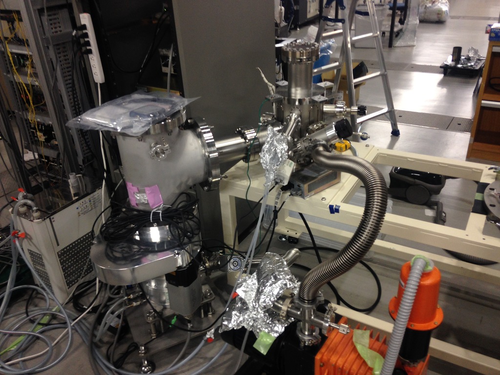
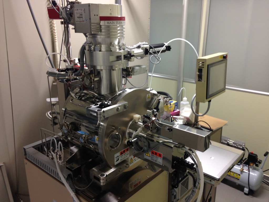
1.Electron beam evaporation (Py, Pt, Pd, Ta, Cu, Au, Ti, Fe, CuNi, Al, AuSb etc.)
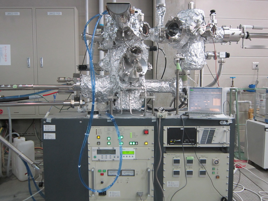
2.Pulse laser deposition (Bi, BiSb, W, Ta etc.)
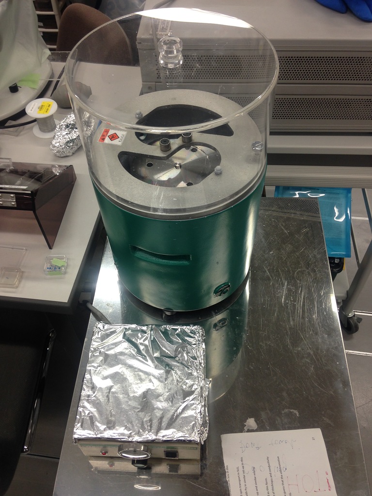
3.Joule heating evaporation system
4.Ar-milling system with end point detection
5.Polishing machine
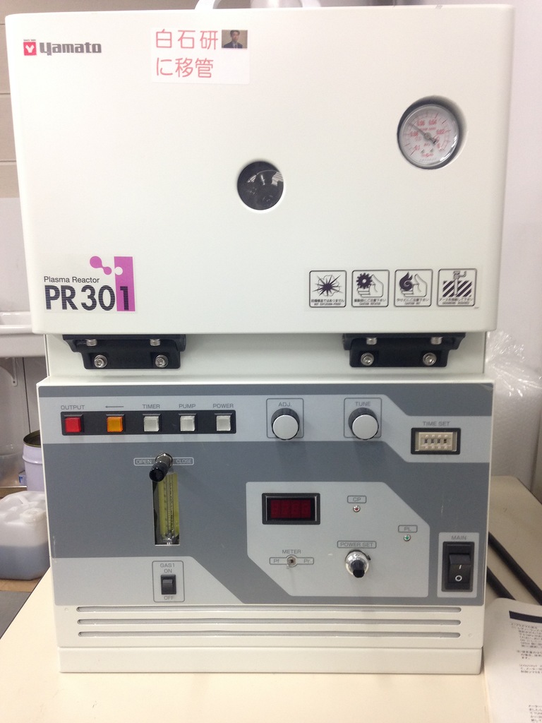
6.Plasma reactor
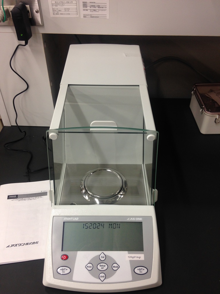
7.Precise digital scale
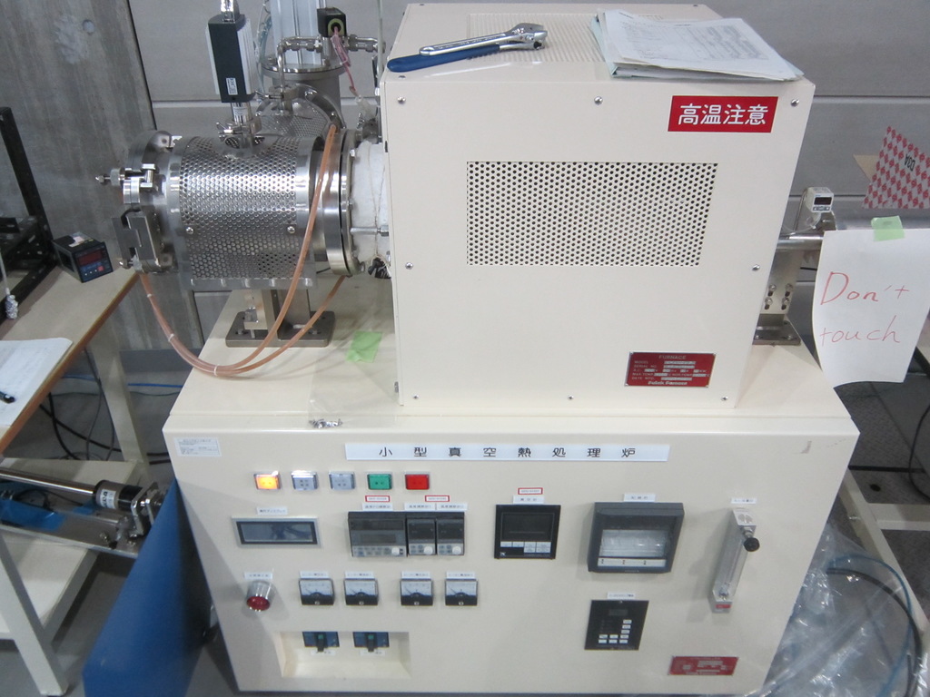
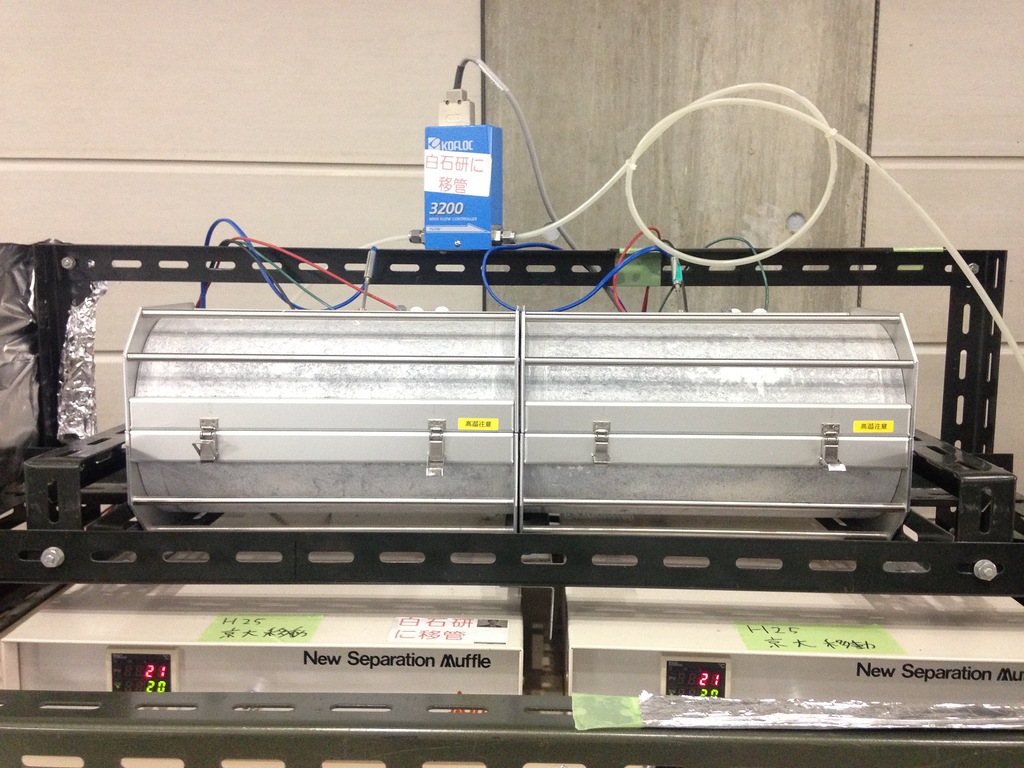
8.Annealing systems up to ~1200 C
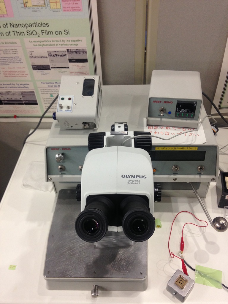
9.Wire bonding
10.Dicing machine
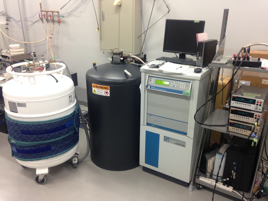
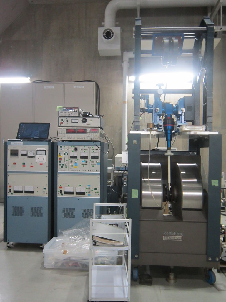
11.Physical Property Measurement System PPMS (1.8 - 297 K, magnetic field up to 9T)
12.Vibrating sample magnetometer
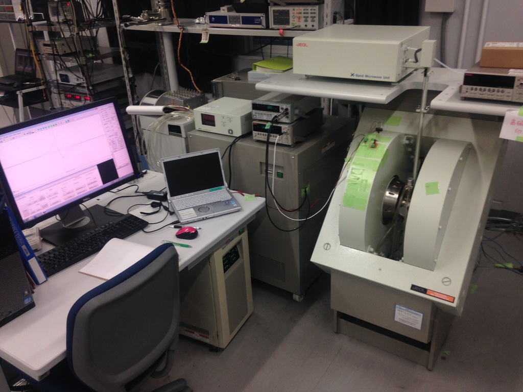
13.JEOL JES-FA200 Electron spin resonance spectrometer (100 - 470 K, 8.75 - 9.65 GHz, magnetic field up to 1.3 T)
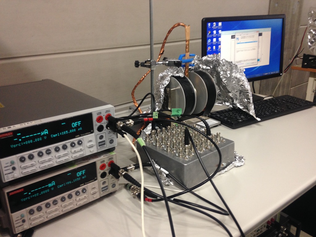
14.Four-probes station with magnetic field (4.2-297 K, magnetic field up to 0.3 T)
15.Four-probes station (4.2-297 K)
16.Thermally-induced spin transport measurement system
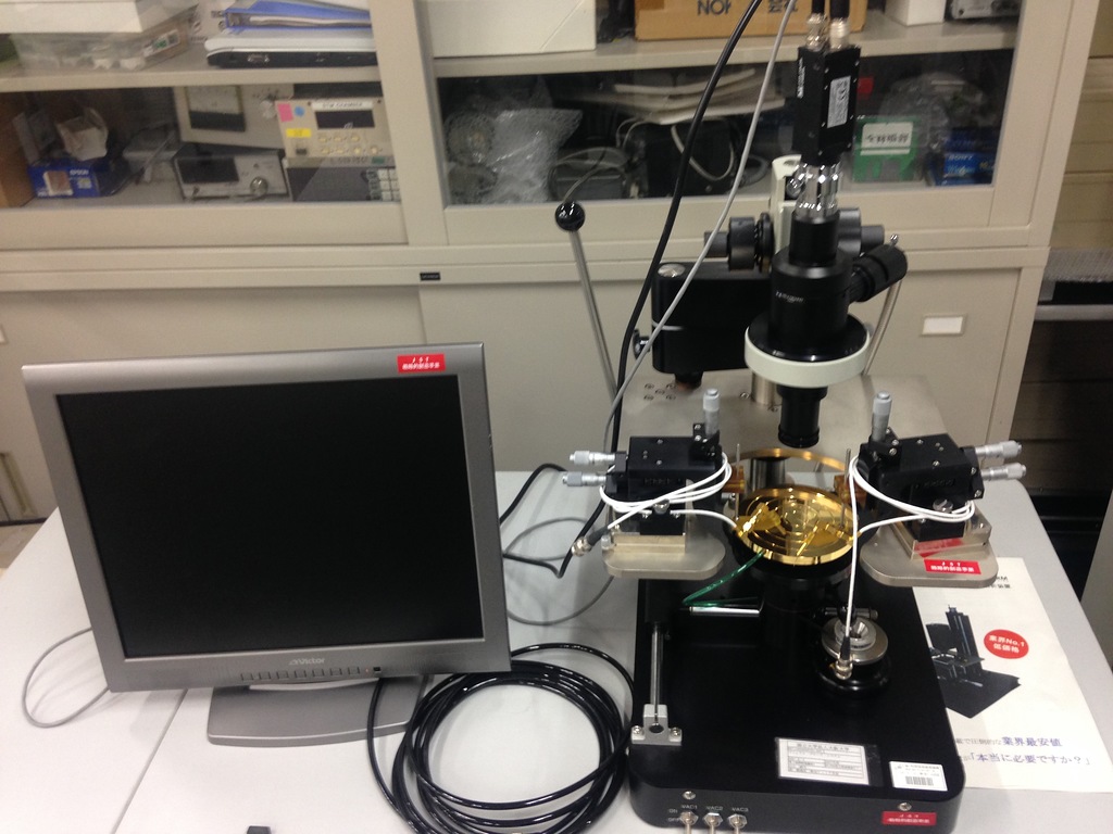
17.Probe station
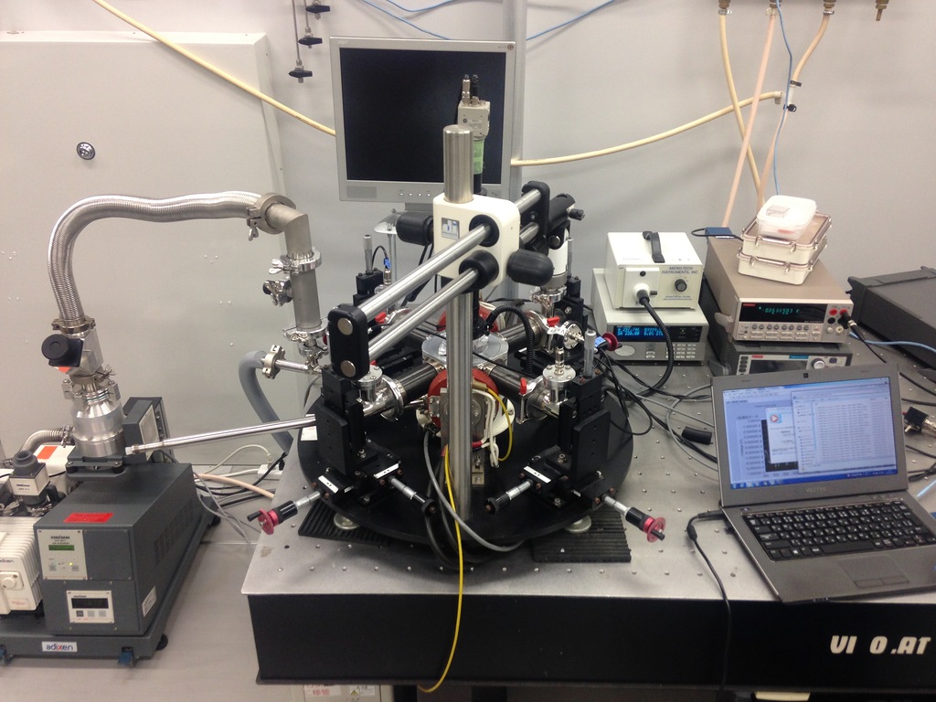
18.Cryostat for spin transport measurements (4.2-297 K, magnetic field up to 1 T)
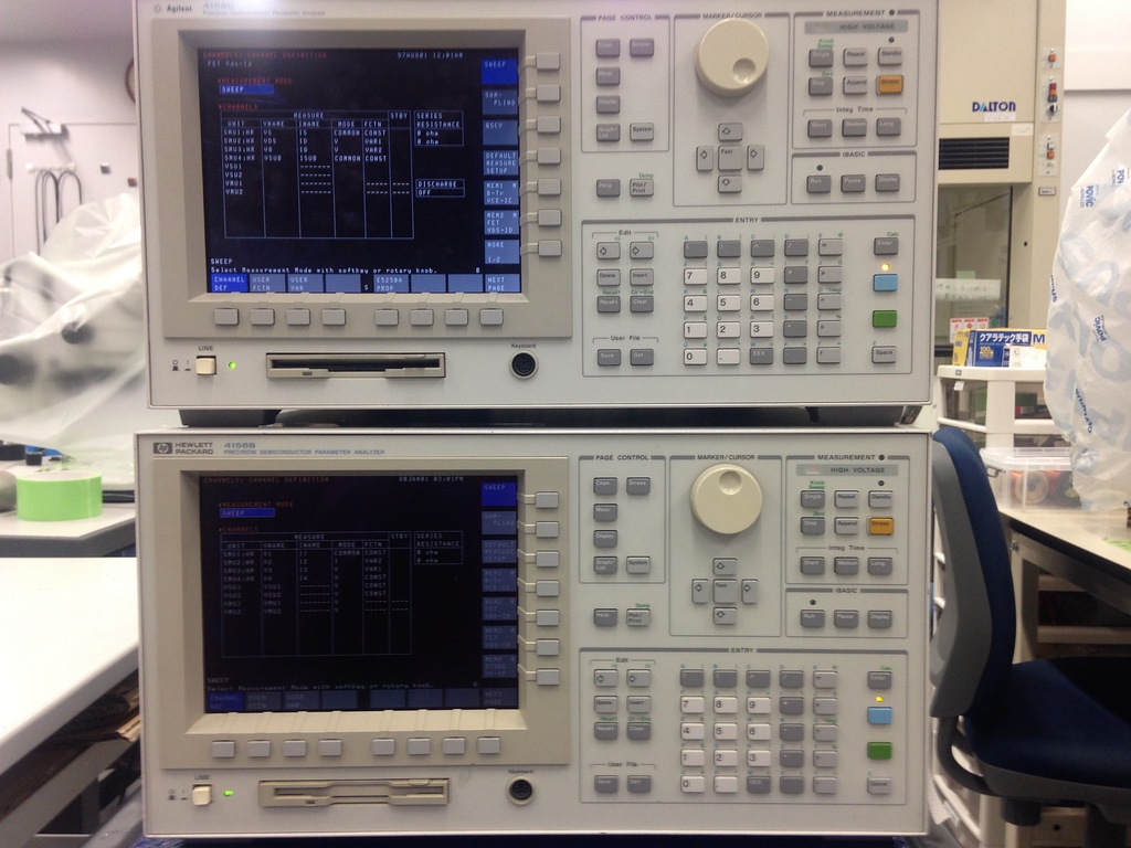
19.Precision Semiconductor Parameter Analyzers
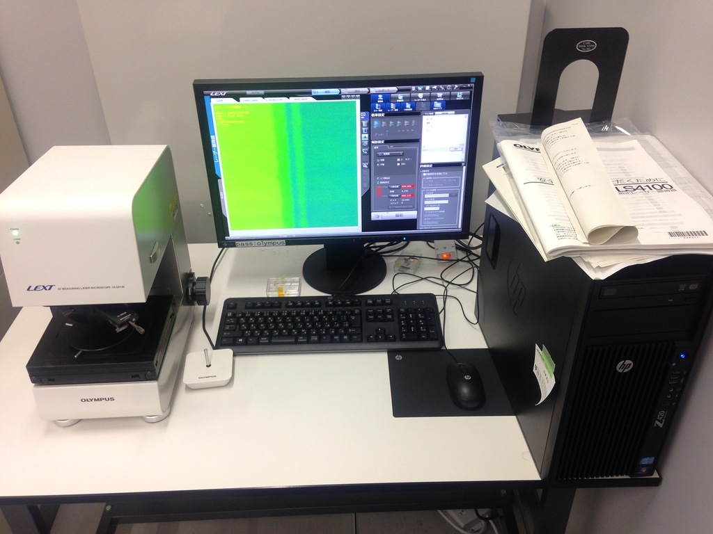
20.Laser microscopy system
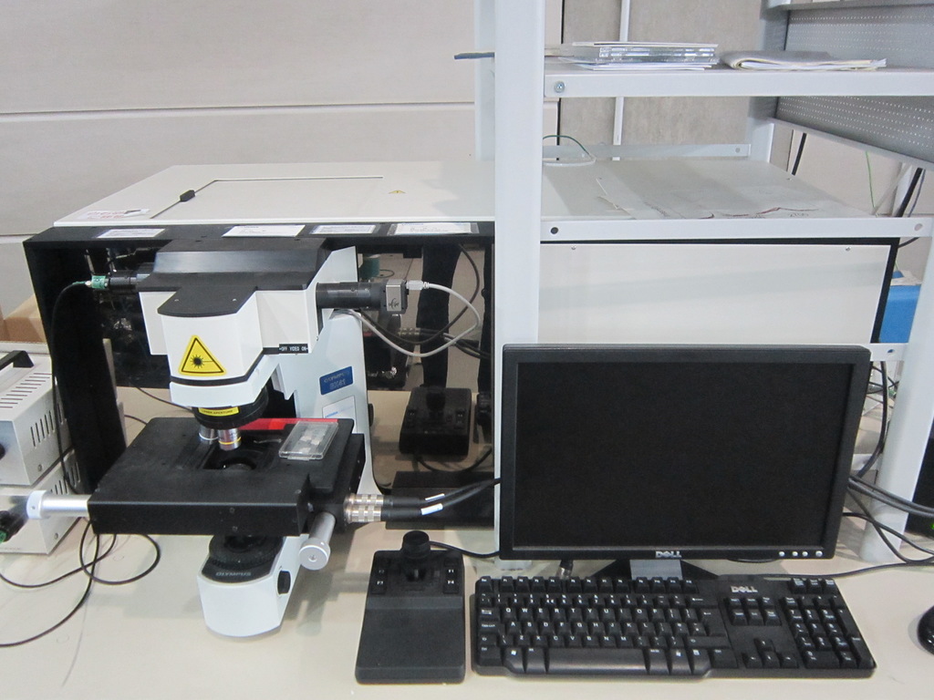
21. Raman spectroscopy system
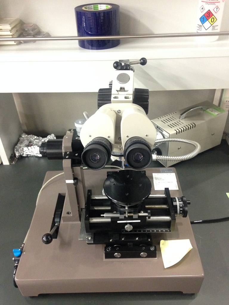
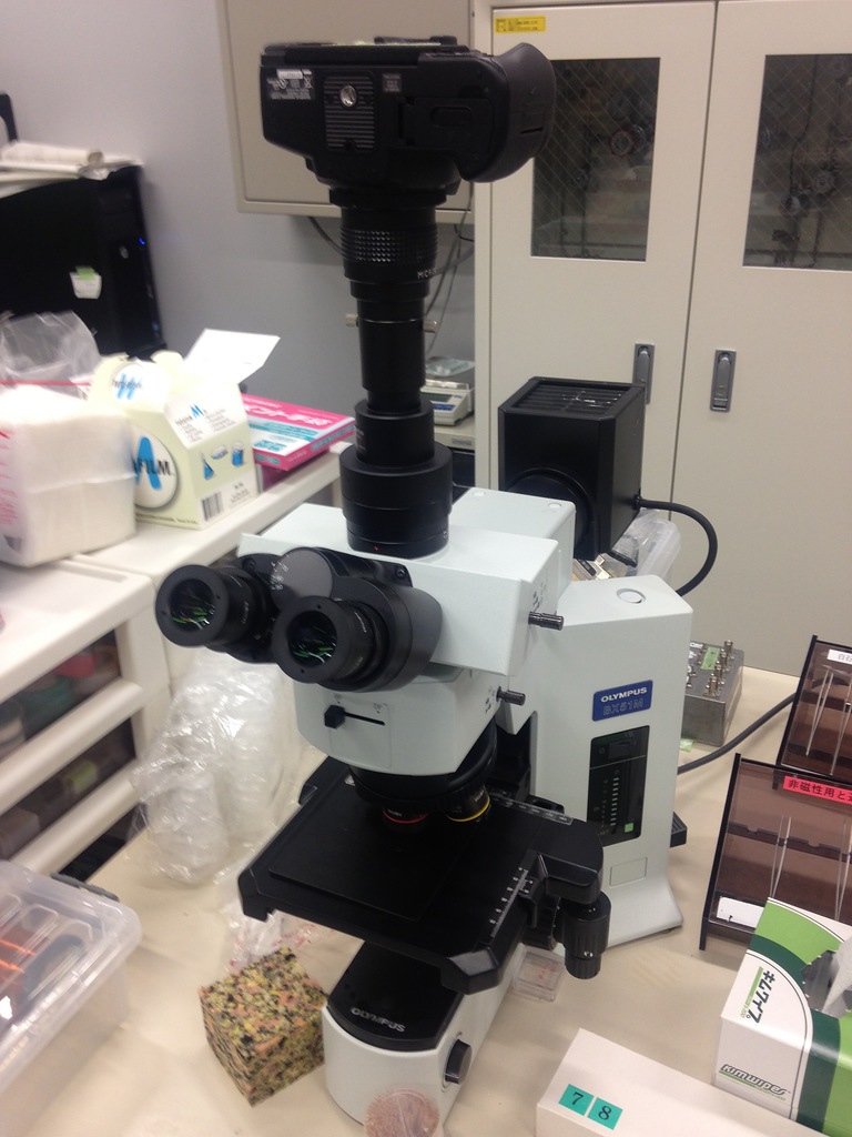
22. Optical microscopes
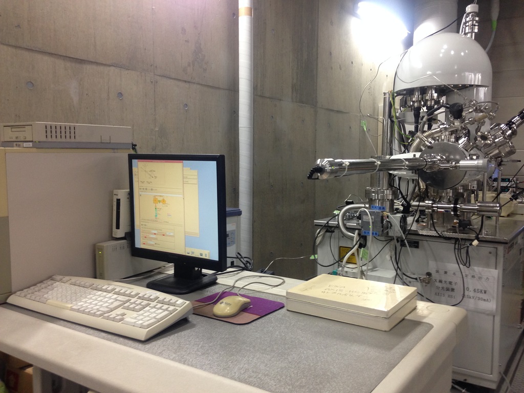
23. X-ray photoelectron spectroscopy
DEVICES